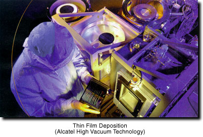

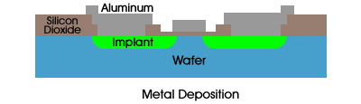
Evaporation uses heat (either an electric filament or an electron beam) and high-vacuum (between 5x10⁻⁵ Torr and 1x10⁻⁷ Torr) to vaporize the metal source. The evaporating source material condenses on the surface of the cooler wafers which are held in a semispherical or "planetary" arrangement over the source.
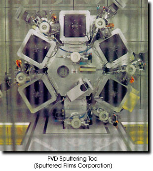
Sputtering uses a cathode to create an argon plasma which bombards the source metal. The dislodged metal molecules are focused by a "lens" of radiation-absorbent material, called a collimator, and deposited in a thin film on the surface of the wafer.