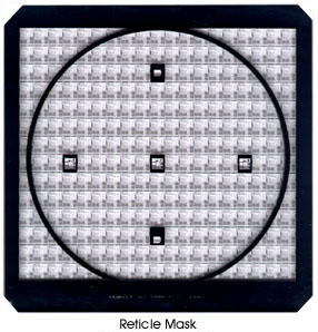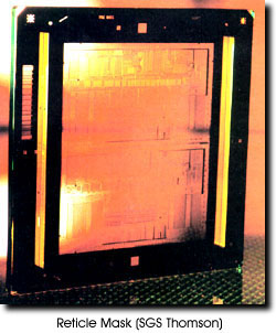

Semiconductor devices are made up of as many as 50 individual layers of silicon, polysilicon, silicon dioxide, metal and silicides, The pattern for each layer is contained on a mask called a reticle. Reticles are between 1 and 10 times the actual size of the pattern they will produce. The group of reticles that make up all the layers of a semiconductor device is called a device series.
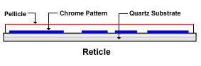
A reticle is an optically clear quartz substrate with a chrome pattern. To keep the surface of the reticle clean, a thin plastic sheet called a pellicle is mounted a short distance away from the surface of the reticle. This allows the wafer to be cleaned without directly contacting the chrome mask surface, but also insures that any microscopic dust that settles on the reticle will be out of focus during exposure and not create defects.
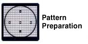
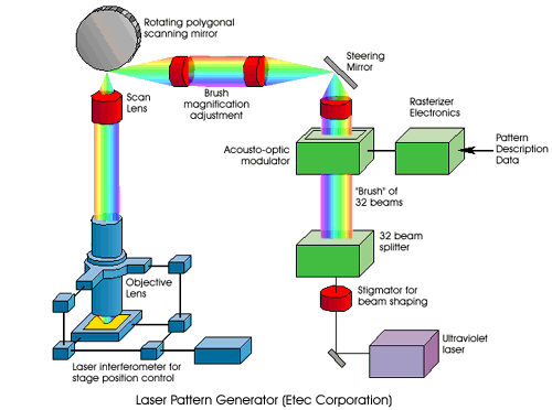
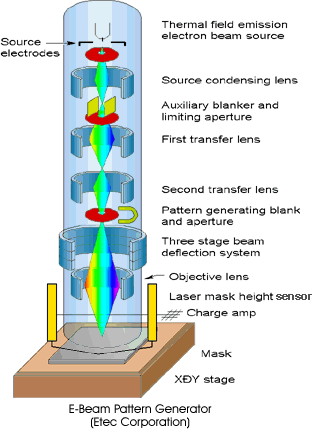
IC designers design the pattern for each layer using CAD software. They then prepare a chrome coated reticle blank and apply a layer of photoresist. The CAD pattern is transferred to the reticle using one of two devices: a laser pattern generator or an e-beam.
After pattern generation, the exposed (acidic) photoresist is removed with a base solution which leaves the unwanted portions of the chrome layer exposed. The chrome is then etched away in an acidic solution of cerric ammonium nitrate. The remaining photoresist is removed with a process called ashing which leaves a clean chrome and quartz surface.