
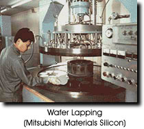
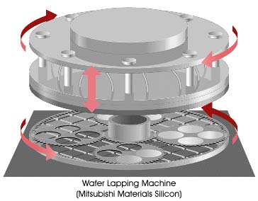
Wafer Lapping
Wafer Etching
After lapping, wafers are etched in a solution of nitric acid/
acetic acid or sodium hydroxide
to remove microscopic cracks or surface damage created by the lapping process. The acid or caustic solution is
removed by a series of high-purity RO/DI water baths.
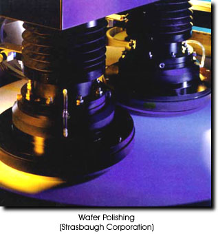
Wafer Polishing
Next, the wafers are polished in a series of a combination chemical and mechanical polishing processes called CMP.
The wafers are held in a hard ceramic chuck using either wax bonding or vacuum and buffed with a slurry of silica powder, RO/DI water and sodium hydroxide.The polishing process usually involves two or three polishing steps with progressively finer slurry and intermediate cleanings using RO/DI water.
Wafer Cleaning
Most wafer manufacturers use a final cleaning method developed by RCA in 1970. The 3-step process starts with an SC1 solution (ammonia, hydrogen peroxide and RO/DI water) to remove organic impurities and particles from the wafer surface. Next, natural oxides and metal impurities are removed with hydrofluoric acid, and finally, the SC2 solution, (hydrochloric acid and hydrogen peroxide), causes super clean new natural oxides to grow up on the surface.