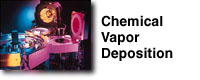

Chemical Vapor Deposition, or CVD is a broad class of processes using controlled chemical reactions to create layers on wafers.
Prior to deposition, the wafer is usually cleaned with a Dry Plasma Etch process using either sulfur hexafluoride or a combination of tetrafluoromethane and oxygen.
The exact "recipes" used by IC manufacturers are some of their most closely guarded secrets but typically, using nitrogen and hydrogen as carrier gases, CVD can produce a variety of layer types. For example, ammonia and dichlorosilane will produce a silicon nitride layer. Silane and oxygen are used to create silicon dioxide layers.
Special hybrids of silicon and metal called silicides can be used to create conductive layers. For example, tungsten hexafluoride is used to create a tungsten silicide layer.
A variant of CVD called Plasma-Enhanced Chemical Vapor Deposition, or PECVD, uses a gas plasma to lower the temperature required to obtain a chemical reaction and achieve film deposition.
Cleaning of CVD chambers is usually done using nitrogen trifluoride plasma.
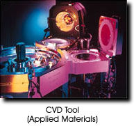
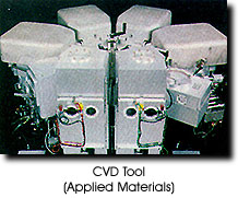
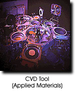
The CVD tools illustrated here are a special kind of multi-chamber CVD tool called a "cluster tool" that can perform multiple sequential operations automatically.