Characterization & Wafer Slicing


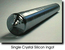
Single crystal silicon ingots are created with a crystal pulling process originally developed by Mitsubishi Materials Silicon called the CZ (Czochralski) method.

Crushed high-purity polycrystalline silicon is doped with elements like arsenic, boron, phosphorous or antimony and melted at 1400° in a quartz crucible surrounded by an inert gas atmosphere of high-purity argon. The melt is cooled to a precise temperature, then a "seed" of single crystal silicon is placed into the melt and slowly rotated as it is "pulled" out. The surface tension between the seed and the molten silicon causes a small amount of the liquid to rise with the seed and cool into a single crystalline ingot with the same orientation as the seed. The ingot diameter is determined by a combination of temperature and extraction speed.

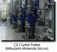
They install the crystal pullers on large concrete foundations (sometimes as large as an 8 foot cube) to control vibration and allow proper crystal orientation and prevent disturbing the creation of surface tension.

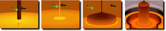
Process piping support systems  include process cooling water (to precisely control heat during the process and allow formation of the "shoulder" that determines the actual ingot diameter) and high-purity argon and vacuum systems to provide a contaminant free atmosphere for the ingot.

Most ingots produced today are 150mm (6") and 200mm (8") diameter, but Komatsu Silicon America, MEMC, Mitsubishi Silicon America, Shin-Etsu Handotai America, and Wacker Siltronics are developing 300mm (12") and 400mm (16") diameter ingots.